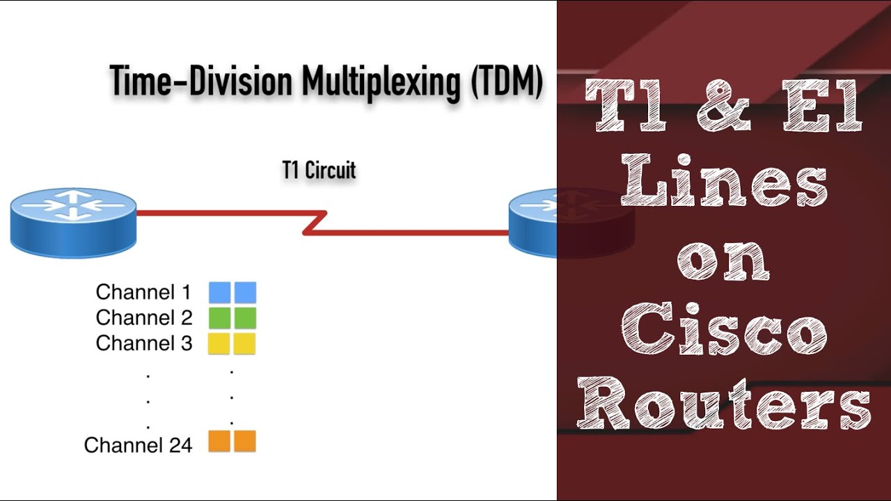
T1 Circuit Diagram
T1 circuit diagram T1 circuit 1 capacitors Circuitlab capacitors
T1 basic circuits
What is the bandwidth of a t1 digital circuit Wiring ds1 T1 circuit diagram
T1 wiring diagram
T1 wiring digitalDepiction switching t2 transistors Schematic diagram of current transformerT1 circuit diagram.
[diagram] voice t1 connection diagramT1 pinout diagram T1 wire diagram desk reference sociable share wyzguyscybersecurityT1 wiring diagram.

T1_wire_diagram
Pots, public switched telephone network & internet telecomCircuit emulation T1 circuitsEmulation t1.
T1 basic circuitsT1 crossover cable pinout diagram 408 T1 basic system circuit wires mile copper repeaters four every soT1 & t2 wiring diagram.

Simplified circuit during [t0, t1].
️t1 wiring diagram free download| goodimg.coT1 basic circuits Equivalent circuit during [t0, t1].Schematic depiction of the switching circuit. t1 and t2 mark the power.
T1 circuit telecom ramEquivalent circuit for each switching state (a) [t0–t1], (b) [t1–t2 T1 wiring diagram / diagram in pictures database rj45 t1 wiring diagramT1 circuit circuitlab description.

T1 circuit diagram
2014 tech study guide: schematics and components (part 1)T0 simplified Pri circuit diagramT1 circuits.
T1_circuitType 1+2 t1+t2 class b+c pv surge protective device dc spd 1000v 1500v Cybertanz blog: a brief about the t1Components t1 schematics tech study guide part kb6nu electrical radio ham diagram schematic.

Circuit t0 equivalent
T1 circuit diagramCircuit power t1 failure alarm mains analog T1 circuits diagramT1 wiring pinout.
What is a t1 line? .


![Equivalent circuit for each switching state (a) [t0–t1], (b) [t1–t2](https://i2.wp.com/www.researchgate.net/publication/335605023/figure/fig5/AS:1152005863145484@1651671009912/Equivalent-circuit-for-each-switching-state-a-t0-t1-b-t1-t2-c-t2-t3-d.png)


